Recent Posts

Blogroll

                                          My PIC12F683 Development Board
Office Map Circuit diagram for each experiment may not be available separately because they are conducted with PIC12F683 development board that I made. So, the readers should first see the schematic of my development board.

Sunday, November 28, 2010

Experiment No. 7: Generating Melody with a Microcontroller

Introduction
This experiment is about generating a melody tune using a PIC microcontroller. Well, this won't be difficult if you know the notes of the tune, and their respective frequencies. Here's a chart for note to frequency conversion. We will play the 'Happy Birthday' tune with a PIC12F683 microcontroller. The microcontroller will generate the frequencies of the various notes (with proper timing) in the tune and the melody will be played in a piezoelectric buzzer.

Circuit Setup
The piezo buzzer is connected to the GP2 port of PIC12F683.

Thursday, October 28, 2010

Contact-less tachometer based on PIC16F628A uC

Check out my new tachometer project based on PIC16F628A microcontroller. It uses an infrared sensor module to sense the rotation speed of a shaft or disc. The range of measurement is 0-9999 RPM. The full details on hardware and software is available.

Sunday, October 3, 2010

0-20V Digital Voltmeter (DVM) using PIC12F683

After finishing the serial LCD project, it is time to do some cool projects using PIC12F683. Now we can have a nice LCD display with PIC12F683. This project shows how to make a digital voltmeter of range 0-20V using PIC12F683. Enjoy!


Background
You cannot feed 20V  directly to a PIC I/O pin, you need a resistor divider network that converts 0-20V range into 0-5V. The figure below shows how it will be achieved.
At any instant, the voltage Va will be 1/4th of the input voltage, Vin. So, for maximum input voltage of 20V, the Va will be 5V. A 5.1V Zener diode in the figure is to prevent Va to rise above 5.1V if the input voltage goes much above 20V. This will protect the microcontroller port. The analog voltage Va is read through AN0 port and is converted to 10-bit digital number (0-1023) by PIC12F683.

Monday, September 27, 2010

Serial LCD for Low Pin-Count PIC Microcontrollers using 74HC595 Shift Register

Introduction

HD44780 based character LCD displays are very popular among hobbyists. They are easy to interface with microcontrollers and most of the present day high-level compilers have in-built routines for them. However, the bad part is at least 6 I/O pins of microcontroller are required to use them in your project. Therefore, they are not applicable for 8-pin devices like PIC12F series microchips. The aim of this project is to allow LCD interfacing to such devices using 3-wires. I am going to demonstrate this with PIC12F683 microcontroller. The character data or command from the microcontroller will be transferred serially to an 8-bit serial-in parallel-out shift register (74HC595), and the parallel output will be fed to the LCD driver pins.

Saturday, September 25, 2010

Experiment No. 6: PIC12F683 Timer1 used as a Frequency Counter

Objective: Determine the frequency of an external clock source (0-65535 Hz), send it to PC through serial port, and display it on a hyperterminal application window.

Introduction

The Timer1 module in PIC12F683 is a 16-bit timer/counter. It can operate as Timer or as a synchronous/asynchronous counter. In asynchronous mode, the Timer1 will increment at the arrival of each external clock pulse at T1CKI port. Whereas, in synchronous mode the input clock pulse to Timer1 module is synchronized to the microcontroller internal clock. A dedicated control register, T1CON, is available to set-up and control the Timer1 module. We are going to use the counter feature of it to measure the frequency of an external clock source. The Timer1 register pair (TMR1H:TMR1L) increments from 0000h to FFFFh and rolls over to 0000h. When Timer1 rolls over, it indicates timer overflow by setting Timer1 interrupt flag (TMR1IF) bit of PIR1 register. To enable the interrupt on rollover, following bits must be set:
  • Timer1 interrupt enable (TMR1IE) bit of PIE1 register (PIE1 = 01h could do that)
  • PEIE and GIE bits of the INTCON register (INTCON = C0h could do that)
Since the 16-bit counter can count up to 65535, the external clock source with frequency higher than this will overflow the Timer1 counter, and generate the Timer1 overflow interrupt. The external clock source will be obtained from a 555 Timer IC operating as an astable multivibrator, and will be fed to GP5/T1CKI pin (2) of PIC12F683. Once I made a 555 experiment board for myself, I am going to use the same. In this board I can vary the frequency of the multivibrator using a potentiometer. Search internet for more detail on 555 astable multivibrator.

My 555 Timer IC Experiment Board

Friday, August 27, 2010

A Versatile Temperature Data Logger using PIC12F683 and DS1820

Introduction
There are varieties of digital temperature logger projects available online based on different microcontrollers. The one I am going to talk about is based on a Microchip's 8-pin microcontroller, PIC12F683. It reads temperature values from a DS1820 digital sensor and stores in its internal EEPROM. PIC12F683 has 256 bytes of internal EEPROM and we are going to store the temperature values in 8-bit format. This means only the eight most significant bits of temperature data from DS1820 will be read and as such the temperature resolution will be of 1 degree C.

My temperature logger has following features:
  • Reads temperature from a DS1820 sensor and stores in the internal EEPROM locations.
  • Can store up to 254 temperature values. EEPROM location 0 is used to store the sampling interval, and location 1 is used to store the number of records.
  • Three sampling interval options: 1 sec, 1 min, and 10 min. This can be selected during powering up.
  • Start and Stop buttons for control operations.
  • The recorded temperature values can be sent to PC through a serial port. A separate Send button is available to initiate data transfer.
  • A LED to indicate various ongoing operations.
  • Reset button to clear all previous records.  

Saturday, July 31, 2010

Experiment No. 5: DC Motor Speed Control using Pulse Width Modulation (PWM)

Introduction

PIC12F683 has a built-in PWM module. The PWM output (CCP1 pin) is multiplexed with GPIO.2 (pin 5). So the TRISIO<2> bit must be cleared to make the CCP1 pin an output.
The objective of this experiment is to control the speed of a DC motor with an input from a potentiometer. This will be achieved in two steps:
  • Read analog value (potentiometer output) through AN0 channel and generate a PWM wave at CCP1 pin (5) with duty cycle proportional to the analog value.
  • Feed the PWM to motor driver transistor and observe the speed.
mikroC library routines for PWM
PWM1_Init
PWM1_Set_Duty
PWM1_Start
PWM1_Stop

Since PWM1_Set_Duty library function takes duty cycle input as an 8-bit integer, the digital value of analog signal, which is 10-bit, must be converted to 8-bit first. This will give 256 speed levels (0-255).

Experimental Setup
Connect POT2 output to pin 7 (AN0) of PIC12F683 and pin 5 (CCP1) to the input of motor driver transistor.

Saturday, June 26, 2010

Experiment No. 4: External Interrupt

PIC12F683 has got one external interrupt pin (GP2, pin 5) which is edge-triggered:
  • rising edge if INTEDG bit in OPTION register is SET,or 
  • falling edge if INTEDG bit in OPTION register is CLEAR
In this experiment we are going to simulate an external interrupt event by a tact switch which when pressed gives a falling edge (5->0V) to external interrupt pin. When a valid edge appears on GP2/INT pin, the INTF bit (INTCON<1>) is set. This interrupt can be disabled by clearing INTE control bit (INTCON<4>). While exiting from the Interrupt Service Routine, INTF flag must be cleared to re-enable the interrupt again. ANSEL and CMCON0 must be initialized to configure GPIO as digital I/Os.

On the arrival of an interrupt, the new value of counter will increase by 1 and is displayed as no. of interrupts serviced. 

Experimental Setup:
External interrupt will be simulated by a tact switch on the board. So connect SW1 to GP2 with a jumper wire. For display purpose we will again use a hyperterminal window on a PC.


Experiment No. 3: Analog to Digital Converter with PIC12F683

As mentioned before, 4 out of 6 GPIOs in a PIC12F683 also provide analog-to-digital converter inputs with 10-bit resolution. They are GP0-GP2, and GP4. In this experiment we will feed an analog voltage to one of the ADC inputs (say AN0, which is GP0) and display the output digital value on a hyper-terminal window on PC. The analog voltage will be simulated with the potentiometer on our board.

Experimental Setup:
Connect the output of potentiometer (POT2) to AN0 (pin 7). GP5 (pin 2) will serve as TX pin for Software UART so connect it to input Tx of TTL to RS232 Level Shifter circuit. Also connect Rx (2) and Gnd (5) of a RS232 port to the board. This is similar to what we did in Experiment No. 2.

Saturday, April 3, 2010

Experiment No. 2: User Inputs from Tact Switches and Software UART

In this experiment, we will demonstrate how to read inputs from tact switches, and then will also show how to send character data from PIC12F683 to a desktop PC Hyper-Terminal program through UART communication. Remember that PIC12F683 doesn't have hardware UART module, so we are going to use the Soft_UART library routines from mikroC for this purpose. Regarding the Hyper-Terminal setup on PC, read this. Besides, to read the user inputs from tact switches, Button Library routines in mikroC will be used.
Snapshots of the required Library Routines from mikroC User's Manual


Setup:
The two switch inputs in our board will be connected to GP0 and GP1 port (Pins 7 and 6 respectively). GP5 (Pin 2) will be used for Software UART Tx. So here is what you need to do:
  • Connect SW1 and SW2 (tact switches) to GP0 and GP1 using jumper wires,
  • Connect GP5 to input Tx of TTL to RS232 Level Shifter circuit,
  • Connect Rx(2) and Gnd(5) pins of a RS232 port to the board.

Saturday, February 13, 2010

Experiment No. 1: 3-bit LED Up Counter

This is the first and the simplest project we are going to test on our PIC12F683 experiment board. We are going to make a 3-bit up counter that counts from 0 to 7. After 7, we are going to reset it to 0 and then start again, and so on. The 3-bit counter output will be displayed on 3-LEDs on the board. There will be a 1s delay between each up count.
Setup:
Connect GP0, GP1, and GP2 (pins 7, 6, and 5 of PIC12F683) to LEDs 3, 2, and 1 respectively.
 
Connect GPIO2, 1, 0 pins to LEDs 1, 2, 3 using jumper wires.

What else you need to start experimenting on this board?

After you finish constructing the development board, here are few more things to do before doing some real experiments with it.

  • Of course, you need a 9V DC adapter for power supply. I sometimes use the power supply from my PIC programmer which derives power from a USB port of my computer. But do this only if you are sure that the experiment you doing draws current which is within the safe limit of the USB port.
  • Next, you also need jumper wires to interconnect the various terminals while doing experiments.
  • It depends on you what kind of platform you want to choose for programming the PIC. If you want to use assembly language, you need to download MPLAB. It is free to download from the Microchip website. You can also find an installation guide for this, which might be helpful. However, I prefer high-level language like C for programming my PIC. I am going to use mikroC compiler from Mikroelektronika for all the experiments I am going to show here. You can download a demo version of this compiler for free. The demo version restricts the output HEX file size to 2K, but we don't care because PIC12683 doesn't have programming memory more than that. So, you decide. 

Friday, February 5, 2010

Make Your Own PIC12F683 Microcontroller Development Board

Our purpose here is to explore the potential of PIC12F683 microcontroller for which we need a development board. The good thing is we are going to make our own board. The schematic and the actual board that I have built are shown below. I soldered all the components on a 12 x 8 cm general purpose prototyping board. 

 
Completed Board

It has following features in it:
1. A Regulated +5V power supply.
2. 3 Output LEDs that can be connected to any GPIO pins using jumper wires.
3. ON/OFF power supply switch.
4. A Green LED as a power ON indicator.
5. An 8-pin IC socket for PIC12F683 microcontroller.
6. Two potentiometers: one for providing Vref, and other for simulating analog input to ADC.
7. An ICSP header connector.
8. Two tactile switches for input operation.
9. A TTL to RS232 level shifter using a transistor circuit.
10. A piezo buzzer.
11. A DC motor with driving circuit.

Thursday, February 4, 2010

PIC12F683: A brief Introduction

PIC12F683 is a 8-pin Flash based,  8bit RISC microcontroller from Microchip. This little PIC microcontroller offers up to 6 I/O pins (the remaining two are power supply pins). It needs no external oscillator, as it has an in-built oscillator with software selectable frequency from 8 MHz to 125 KHz. It also offers a feature that allows external signals to wake it upfrom the sleep state. Here are the various features as mentioned on the datasheet.


High-Performance RISC CPU:
• Only 35 instructions to learn: All single-cycle instructions except branches
• Operating speed:
 - DC – 20 MHz oscillator/clock input
 - DC – 200 ns instruction cycle

• Interrupt capability
• 8-level deep hardware stack
• Direct, Indirect and Relative Addressing modes

Special Microcontroller Features:
• Precision Internal Oscillator:
 - Factory calibrated to ±1%, typical
 - Software selectable frequency range of 8 MHz to 125 kHz
 - Software tunable
 - Two-Speed Start-up mode
 - Crystal fail detect for critical applications
 - Clock mode switching during operation for power savings

• Power-Saving Sleep mode
• Wide operating voltage range (2.0V-5.5V)
• Industrial and Extended temperature range
• Power-on Reset (POR)
• Power-up Timer (PWRT) and Oscillator Start-up Timer (OST)
• Brown-out Reset (BOR) with software control option
• Enhanced Low-Current Watchdog Timer (WDT) with on-chip oscillator (software selectable nominal 268 seconds with full prescaler) with software enable
• Multiplexed Master Clear with pull-up/input pin
• Programmable code protection
• High Endurance Flash/EEPROM cell:
 - 100,000 write Flash endurance
 - 1,000,000 write EEPROM endurance
 - Flash/Data EEPROM Retention: > 40 years


Peripheral Features:
• 6 I/O pins with individual direction control:
 - High current source/sink for direct LED drive
 - Interrupt-on-pin change
 - Individually programmable weak pull-ups
 - Ultra Low-Power Wake-up on GP0

• Analog Comparator module with:
 - One analog comparator
 - Programmable on-chip voltage reference (CVREF) module (% of VDD)
 - Comparator inputs and output externally accessible

• A/D Converter: 10-bit resolution and 4 channels
• Timer0: 8-bit timer/counter with 8-bit programmable prescaler
• Enhanced Timer1:
 - 16-bit timer/counter with prescaler
 - External Timer1 Gate (count enable)
 - Option to use OSC1 and OSC2 in LP mode as Timer1 oscillator if INTOSC mode selected
• Timer2: 8-bit timer/counter with 8-bit period register, prescaler and postscaler

• Capture, Compare, PWM module:
- 16-bit Capture, max resolution 12.5 ns
- Compare, max resolution 200 ns
- 10-bit PWM, max frequency 20 kHz
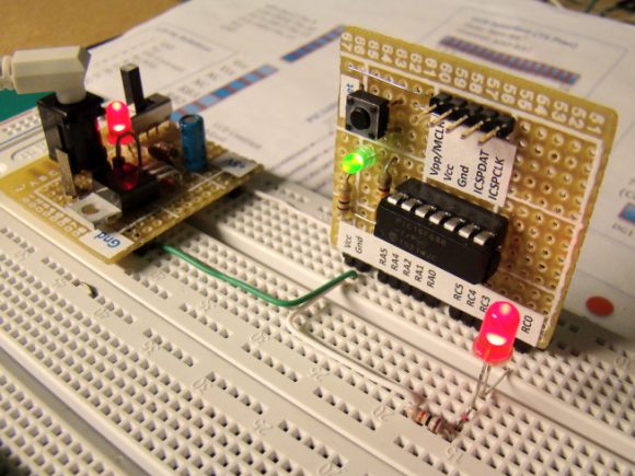
• In-Circuit Serial Programming™ (ICSP™) via two pins


The I/O port of PIC12F683 is called the GPIO (general purpose input/output file register), and the corresponding data direction register is TRISIO. It works mostly the same way as ports in other PIC microcontrollers. Setting a TRISIO bit (= 1) will make the corresponding GPIO pin an input, and clearing the TRISIO bit (= 0) will make it an output. One important thing to note is that GP3 is input only pin, and cannot be configured as an output.

PIC12F683 has a 13-bit program counter that can address up to 8K x 14 program memory, but only the first 2K x 14 (0000h-07FFh) is physically implemented. PIC12F683 also has 256 bytes of data EEPROM with an address range from 0h to FFh.
For details, read the datasheet.

Online Embedded Systems Lab

This online laboratory teaches you the fundamentals of microcontroller-based embedded system development through a series of laboratory exercises. Most of the time, students and hobbyists could not afford expensive development kits and software to learn these things. These tutorials are prepared such that you will be building microcontroller projects at a minimum cost. Check this out