Recent Posts

Blogroll

                                          My PIC12F683 Development Board
Office Map Circuit diagram for each experiment may not be available separately because they are conducted with PIC12F683 development board that I made. So, the readers should first see the schematic of my development board.

Saturday, June 26, 2010

Experiment No. 4: External Interrupt

PIC12F683 has got one external interrupt pin (GP2, pin 5) which is edge-triggered:
  • rising edge if INTEDG bit in OPTION register is SET,or 
  • falling edge if INTEDG bit in OPTION register is CLEAR
In this experiment we are going to simulate an external interrupt event by a tact switch which when pressed gives a falling edge (5->0V) to external interrupt pin. When a valid edge appears on GP2/INT pin, the INTF bit (INTCON<1>) is set. This interrupt can be disabled by clearing INTE control bit (INTCON<4>). While exiting from the Interrupt Service Routine, INTF flag must be cleared to re-enable the interrupt again. ANSEL and CMCON0 must be initialized to configure GPIO as digital I/Os.

On the arrival of an interrupt, the new value of counter will increase by 1 and is displayed as no. of interrupts serviced. 
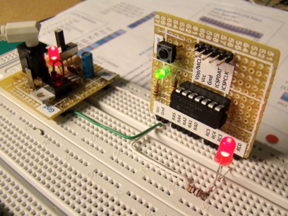
Experimental Setup:
External interrupt will be simulated by a tact switch on the board. So connect SW1 to GP2 with a jumper wire. For display purpose we will again use a hyperterminal window on a PC.


Experiment No. 3: Analog to Digital Converter with PIC12F683

As mentioned before, 4 out of 6 GPIOs in a PIC12F683 also provide analog-to-digital converter inputs with 10-bit resolution. They are GP0-GP2, and GP4. In this experiment we will feed an analog voltage to one of the ADC inputs (say AN0, which is GP0) and display the output digital value on a hyper-terminal window on PC. The analog voltage will be simulated with the potentiometer on our board.

Experimental Setup:
Connect the output of potentiometer (POT2) to AN0 (pin 7). GP5 (pin 2) will serve as TX pin for Software UART so connect it to input Tx of TTL to RS232 Level Shifter circuit. Also connect Rx (2) and Gnd (5) of a RS232 port to the board. This is similar to what we did in Experiment No. 2.

Online Embedded Systems Lab

This online laboratory teaches you the fundamentals of microcontroller-based embedded system development through a series of laboratory exercises. Most of the time, students and hobbyists could not afford expensive development kits and software to learn these things. These tutorials are prepared such that you will be building microcontroller projects at a minimum cost. Check this out